Microelectronic Analog Circuit Design
Homework #1
deadline: 19/10/2009, Monday.
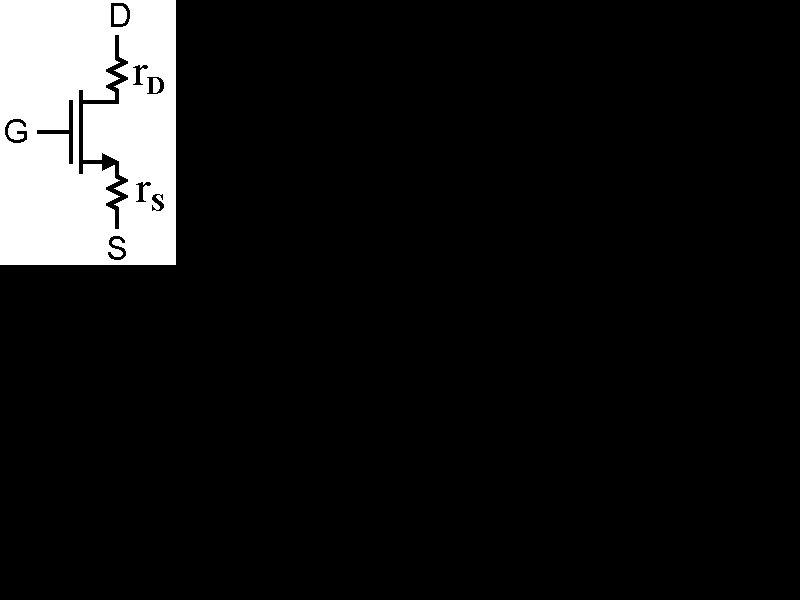
The drain and source body resistances of an n-channel MOSFET
can be represented as shown in the figure below.
1. What are the physical origins of these non-zero body resistances?
2. In analog applications, the effect of the source body resistance
on the performance is much greater with respect to the effect of the
drain body resistance. Why?
3. Give at least two specific drawbacks associated with the large
source body resistance of a MOSFET to be used in an amplifier stage.
4. What are the precautions that can be taken at the "layout drawing
stage" to keep the source body resistance as small as possible?