Low-Voltage Analog Integrated Circuit Design
Design Project #1
Deadline : December 3rd, 2009, Thusday
Two constant-Gm rail-to-rail CMOS input stages will be designed and simulated.
(You can learn the circuits you will design, from the list at the bottom of this page)
Both input stages will be operated from a single 3V supply.
Nominal value of the equivalent small-signal transconductance will be GmT = 250 uA/V.
You can choose and use the model parameters (an adequate model is
preferred) of a suitable CMOS process and an appropriate simulator.
Try to obtain the GmT-ViCM curve with as little ripple as possible.
Also, try to keep the power consumption as small as possible for the worst case.
(It is very likely that, there will possibly be a "worst-case ViCM" for which the power consumption is maximum).
In your project report, explain the methodology you tracked during the design and simulation processes.
You must present the important simulation results (Especially the GmT-ViCM and PDD-ViCM curves) to clearly show the functionality of the circuits you designed.
Don't forget to explain the difficulties you coped with
during the design/simulation processes and explain (or try to guess)
the possible causes of those difficulties.
For convenience, during simulations, you can connect the output current paths (drain terminals) of the nMOS input pair to VDD and those of the pMOS input pair to GND.
When you complete all simulations, force VDD towards lower values and determine the minimum supply voltage value, for which your circuit still operates.
WHO is designing WHICH circuits ?
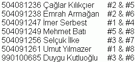
# 1 : The circuit on page 38 of the handouts
# 2 : The circuit on page 41 of the handouts
# 3 : The circuit on page 43 of the handouts
# 4 : The circuit on page 46 of the handouts
# 5 : The circuit on page 48 of the handouts
# 6 : The circuit on page 52 of the handouts
# 7 : The circuit on page 53 of the handouts
# 8 : The circuit on page 55 of the handouts